
2 MHZ MODULATED PHOTOTHERMAL IMAGING USING A CCD
CAMERA COUPLED TO A MULTICHANNEL LOCK-IN DETECTION
S. Grauby, B.C. Forget,
and D. Fournier
We have developed a new photothermal microscope from which we can make
a thermal image of an electronic component working at a "high frequency"
(2 MHz) using a CCD camera and a multichannel lock-in scheme. To do this,
we have created an electronic "stroboscope" which controls the device,
the LED that illuminates the device and analyzes the signal reflected
back to the camera whose amplitude is proportional to the variation of
reflectivity, and hence to the variation of temperature, at the surface
of the device. A thermal image of resistors will be presented.
EXPERIMENTAL SET UP
Most thermal mappings are made using an infrared camera. The spatial
resolution is therefore limited by refraction to the wavelength of the
infrared radiation and, moreover, only a DC or a low frequency thermal
map is obtained. The new method developed in our laboratory overcomes these
drawbacks. The set up couples a classical commercial microscope [1] and
a CCD camera to make a thermal mapping of microelectronic biased devices
illuminated by visible light. In this case, the sample itself serves as
a modulated heat source. This implies a modulated variation of reflectivity
DR which is measured by reflecting an intensity modulated visible light
source (LED) on the surface of the sample and extracting the signal using
a multichannel lock-in scheme.
Let us apply a sine excitation with pulsation wp to a resistor; the
temperature rise of the resistor is then proportional to the dissipated
power, thus to the square of the applied voltage. The pulsation of the
thermal signal will then be 2wp.
Using a pulsation ws=2wp+W
for the modulation of the LED, the flux of the reflected signal can therefore
be written:
f1/2(1+cos(wst+y))(
R0(x,y)+R1(x,y) cos(2wpt+j(x,y)).
We detect the W pulsation signal (heterodyne
detection) on the camera; this term can be written:
f1/4 ´R1(x,y)cos(Wt+y-j(x,y))
The four main elements of the set up are:
- the microscope.
- the LED: l=660 nm and Imax= 20mA. We supply the LED with a
sine signal at the frequency fs=2 MHz + 10 Hz with a sine signal.
- the electronic sample: in our case, the component under investigation
is a polycrystalline Si resistor (a few kW )
modulated at fp=1 MHz with a sine signal (without offset) whose
peak to peak amplitude can be chosen between 0 and 60V.
- the DALSA CCD camera: 40 frames per second, i.e. 4 times the
heterodyne frequency.
The three signals (camera control, LED and device "excitation") are
synchronous. In this manner, we have created a sort of electronic "stroboscope"
since the signal we want to analyze is the one resulting from the blinking
between the two "high" frequencies (2MHz+10Hz for the LED and 2MHz for
the thermal signal on the resistor). The signal of synchronization of the
camera being at 40 Hz, i.e. four times the frequency of the blinking (10
Hz), we will take four images of the component over the blinking period
2p/W. We can show [2] that combining mathematically
these four images, we can extract the amplitude R1(x,y) and
the relative phase y-j(x,y)
of the photothermal signal but also the DC term.
We can note that the choice of 2 MHz as the frequency of modulation
has been arbitrary. The important thing is to have a difference of frequencies
- the frequency of the blinking- low enough to be compatible with the use
of the camera (up to 200 frames per second). So, we can obtain a good spatial
resolution by using a high modulation frequency and visible light.
PRELIMINARY RESULTS
| To validate this lock-in scheme, we have first made an optical experiment
with two light emitting diodes. The technique is very simple: we sum two
synchronous "high frequency" (2MHz and 2MHz+10Hz) TTL signals and supply
a LED with this new "sum" signal. As the LED is a non-linear component,
the current and then the emitted flux- through it presents a term at
the difference of the two frequencies, 10Hz. If we supply another LED with
a continuous voltage ( 5V for instance) and if we combine our four images,
we can see, as expected, that there is only one LED appearing on the image
of the modulated signal but both of them on the DC one.
To evaluate the influence of the accumulation of images, we have analyzed
the noise in the image. Let us take a part of the image where we only have
noise; if we calculate the mean and the standard deviation, we can note
that the mean tends to zero and that the standard deviation is inversely
proportional to the square root of the number of images. This is expected
for additive gaussian noise. So we have a great interest in accumulating
a great number of images; 8000 images could be a good compromise with the
time spent to accumulate (3' 20" in this case). We trace the curve (Fig.1)
of the standard deviation of the real part of the noise versus the number
N of accumulated images and note that the variation is in 1/ÖN. The
imaginary part of the noise has the same property.
|
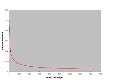 FIGURE 1. Standard deviation of the real part of the noise
versus the number of images
FIGURE 1. Standard deviation of the real part of the noise
versus the number of images
|
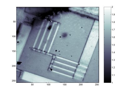
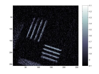
PHOTOTHERMAL IMAGE
We can now use our set-up in the best conditions, making an accumulation
of about 8000 (200sec) images for each measure. The electronic device under
investigation is constituted of two series of four parallel strips of polycrystalline
Si, the ensemble forming a 2.5kW resistor. We have applied them the 1MHz
voltage and lighten them with the modulated LED at 2MHz+10Hz.
We present below the DC image of the electronic device (Fig.2) and
the logarithmic amplitude of the photothermal signal (Fig.3) that leads
to a DR/R» 5.10-3. Of course, as it was expected, we can see that
only the resistor appears in this second figure. The unit of the x and
y scales is the pixel.
|
|
|
FIGURE 2. DC image (arbitrary units)
|
FIGURE 3. logarithmic amplitude of the photothermal signal DR (arbitrary
units)
|
CONCLUSION
We have created a set-up that enables to make thermal mappings using
a CCD camera- of devices working at 2 MHz. At the moment, our signal to
noise ratio is about 10. To improve it, we could envisage to accumulate
more images or to use image processing techniques.
REFERENCES
1. Opsal, J., Rosencwaig, A., and Wilenborg, D. L., Applied Optics 22,
no. 20, 3169-3176 (1983).
2. Gleyzes, P., Guernet, F., and Boccara, A. C., J. Optics (Paris)
26, no. 6,.251-265 (1995).
3. Forget, B. C., Grauby, S., Fournier, D., Gleyzes, P., and Boccara,
A. C., Electronics Letters 33, no. 20, 1688-1689 (1997).
Team / Equipe de recherche :
S. Grauby, B.C. Forget,
D. Fournier
Research topics / Thème de recherche : Photothermy
Return to the top/ Retour
à la page principale